What does it do?
It solves the problem of connecting to millions of wires,
and then using them.
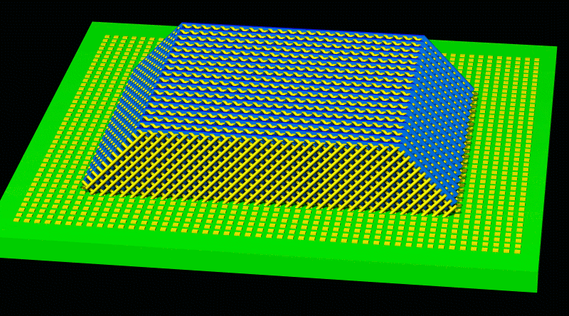
The main novelty is cutting a stack of memory planes diagionally, so that all their wires are accessible on one side, and then using an integrated circuit to connect to those wires.
Why not just build the IC as a stack of planes?
That is expensive and difficult. Only a few planes can be built in
practice that way. Not thousands, like in memory planes made from f.ex.
cheap thin film.
Then why not just make the whole memory device of a roll of thin
film?
Because that memory roll would need some way of connecting to all its
wires, just like IC memories it would need addressing circuitry, and
this is costly, because it needs precise and complicated
manufacturing.
This dense diagonal memory just needs something as simple as crossing
wires in a memory material. This can be made far cheaper. The IC does
the job of addressing.
Getting those diagonal wires to match the pads on the IC seems to
be difficult. It would require precision.
They do not have to match, so precision is not necessary.
Just put them on the IC, and most of them will hit at least one
pad. Multiple connections is not a problem, because in most cases they
will not destroy access to memory segments, and the loss of a few
percent of the elements is a small loss.
The IC can test the pads to see how they are connected to the cross
wires, and then use them.
Amazing.
Yes. And it also means that the layers do not have to be precisely
aligned either, since the IC can map them anyway. The same goes for
the cut as well. The layers could even be bent.
So, it is sufficient to stack memory layers sloppily, cutting
likewise, and sticking it carelessly on the IC for it to work?
Yes. And with error correcting methods, it does not even have to be
done in a clean room, since dirt between the IC and the layers just
means that a small part of the memory is inaccessible.
Sounds like it can be assembled by cheap labour.
Yes, and the memory films can be made sloppily as well, since
variations in the thickness of the wires, thickness of film, bent
wires, variable memory material, etc, all can be compensated for by
using error correcting methods, which have become extremely good now,
in 2006. And they can of course correct errors in the IC as well.
Does all this tolerance of errors and sloppiness cost much in
performance?
No. All kinds memory devices today use error correction anyway, and
tough correction methods are quite fast and use little memory.
As for the speed of this device, the diagonal cut means that all the
memory wires are short, giving them small impedance, less crosstalk,
and thus more speed and less use of energy. The wires are shorter
than in memory ICs.
How large are these memories?
A 100 to 1000 times current flash technology seems reasonable to
expect, with the same size of the IC and packaging.
Is it patented?
Yes, but it is not that hard or expensive to buy.
Snailmail address:
Kim Øyhus
Odvar Solbergs vei 90, L.8013
N-0970 Oslo
Norway